Industrial-grade precision platforms engineered for tracking, compliance, and automated SMT assembly integration.
Malaysia is currently positioned as a crucial node in the global semiconductor assembly, testing, and packaging (OSAT) sector, commanding approximately 13% of the global market share. The economic zones surrounding Kuala Lumpur and Selangor (Klang Valley) are transforming rapidly from traditional assembly plants to high-tech smart manufacturing nodes.
As international consumer electronics manufacturers, automotive electronic component giants, and IoT hardware developers build state-of-the-art facilities in Kuala Lumpur, the requirements for quality control have reached unprecedented heights. Advanced component identification, trace-recording, and anti-counterfeiting practices are no longer optional—they are mandatory.
This industrial evolution creates a massive local demand for reliable, high-speed PCB Laser Marking Machines. High-Density Interconnect (HDI) PCBs, multilayer flexible circuits, and leadframes manufactured in KL require high-fidelity QR codes, barcodes, and serial markings that can withstand heat, soldering fluxes, and severe industrial processing environments.
Hangzhou Kinray Laser Co., Ltd. represents the peak of Chinese laser engineering efficiency, innovation, and technological integration. Our proximity to the global electronics supply chain hub in China gives us an unparalleled R&D cycle time and component sourcing advantage. We pass these cost benefits, quality gains, and innovations directly to the Kuala Lumpur assembly market.
Buying directly from a China manufacturer ensures that you skip domestic markup margins and receive direct technical engineering support. From standard offline desktop UV laser marking setups to custom inline, dual-track CO2 and MOPA fiber configurations, our factory equips your production line with the absolute best in class technology, built to meet stringent international standards (CE, FDA, and FCC).
Tailored laser configurations matching the production realities of electronic manufacturers across Klang Valley.
Marking heat-resistant ceramic, high-density substrate, and metal-clad PCBs for automotive ECUs. Ensuring full track-and-trace throughout the product life under the engine hood.
Precision UV laser engraving for flexible PCB (FPC) boards. Provides cold marking ablation to ensure thin copper traces and polyimide materials remain pristine and free of thermal warping.
Delivers high contrast, corrosion-proof, biocompatible permanent marks for high-precision PCB controllers inside life-support systems, ventilators, and surgical instruments.
In modern manufacturing, traceability is no longer just a trend—it is a regulatory prerequisite. ISO 9001, AS9100, and IATF 16949 standards mandate that electronics manufacturers establish end-to-end component visibility. From assembly line intake to product disposal, components must have a clear identity.
Our laser marking solutions utilize advanced software platforms supporting DXF, AI, DWG, PLT, and BMP formats. This allows SMT operators in KL to easily import complex schematic layouts and sync the laser marker dynamically with their internal MES (Manufacturing Execution System) databases. Dynamic serializing, automatic QR generation, and optical vision inspection features ensure error-free automation cycles.
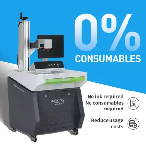
Furthermore, standard ink-based printing systems are rapidly phasing out due to high consumable costs, messy setups, and ink durability issues under heavy solvent washings. Laser marking represents a sustainable, green, permanent, and cost-effective alternative for forward-looking KL electronics plants.
From single desktop workstations to high-throughput fully automated dual-track SMT systems.
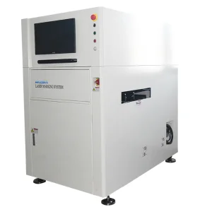
Standard SMEMA signal interface enables seamless connection up and down the production line. Feed boards continuously from solder paste printers directly through the laser marking phase to pick-and-place systems without human intervention.
Handle distinct boards on different tracks simultaneously. Save line space, lower machine overhead, and maximize yield output. Configurable with CO2 or UV laser heads depending on the PCB material properties.
High-resolution integrated cameras detect fiducial marks on boards to automatically orient coordinate offsets. The system self-corrects for position skewing before firing, ensuring perfect alignment every time.
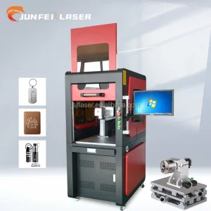
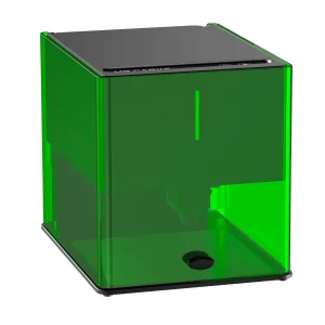
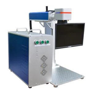
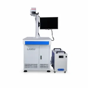
Choose from our broad spectrum of high-performance laser models, configured specifically for industrial electronic parts manufacturing.

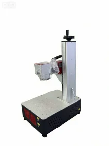
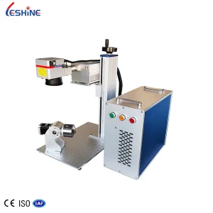
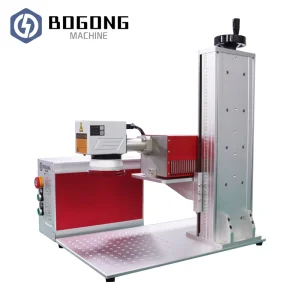
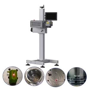
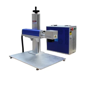
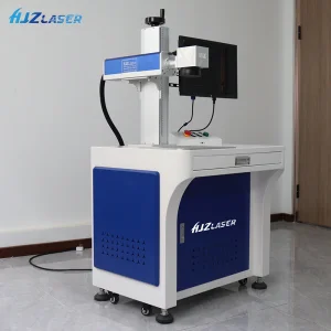
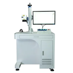
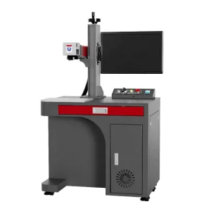
Hangzhou Kinray Laser Co., Ltd. is a leading China industrial laser marking machine manufacturer specializing in advanced fiber and UV laser solutions for global manufacturing industries. With a strong focus on innovation, precision, and intelligent manufacturing, Kinray Laser is committed to delivering high-performance laser equipment that improves production efficiency, product traceability, and marking quality.
Located in Hangzhou, China, the company integrates research and development, manufacturing, sales, and technical support to provide comprehensive laser processing solutions for customers worldwide. Our extensive product portfolio includes fiber laser marking machines, UV laser marking machines, CO2 laser marking systems, MOPA laser markers, flying laser marking machines, 3D laser marking equipment, and customized automated laser solutions.
Kinray Laser products are widely used in electronics, automotive, medical devices, precision hardware, jewelry, packaging, aerospace, consumer goods, and industrial manufacturing industries. Designed for high-speed, high-precision, and permanent marking applications, our systems are capable of processing a wide range of materials, including metals, plastics, ceramics, glass, and composite materials.
Equipped with advanced production facilities and rigorous quality management systems, Kinray Laser maintains strict quality control throughout every stage of manufacturing. Each machine undergoes comprehensive testing to ensure stable performance, reliability, and compliance with international standards.
To support global customers, we offer flexible OEM and ODM services for distributors, system integrators, equipment brands, and industrial manufacturers. Our experienced engineering team works closely with customers to develop customized laser solutions tailored to specific production requirements, automation needs, and industry applications.
Driven by technological innovation and customer satisfaction, Hangzhou Kinray Laser Co., Ltd. continues to expand its global presence and strives to become a trusted partner for intelligent laser processing solutions, helping manufacturers achieve smarter, more efficient, and sustainable production.
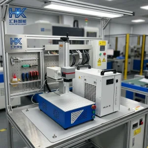
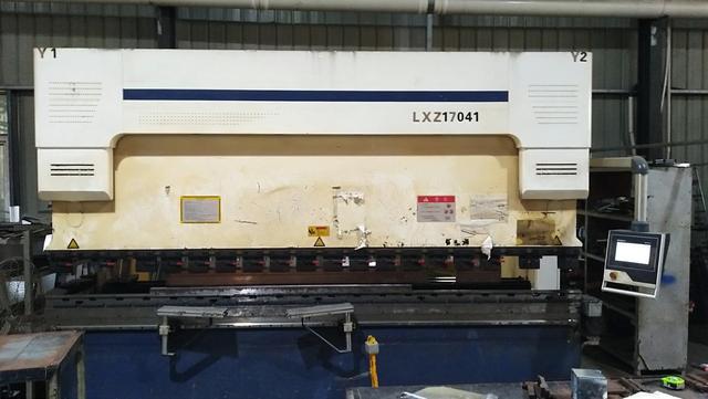
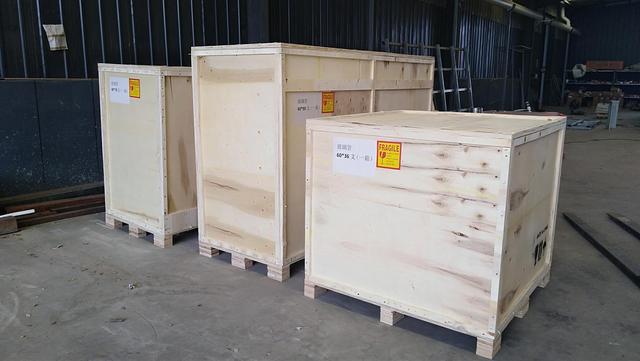
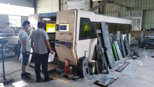
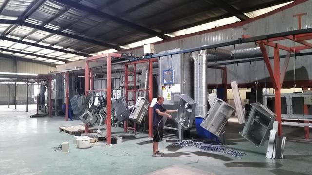
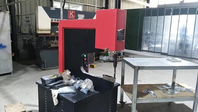
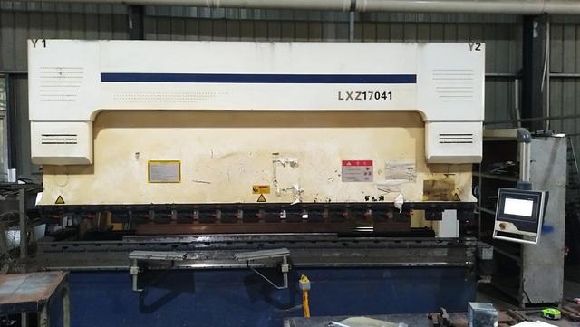
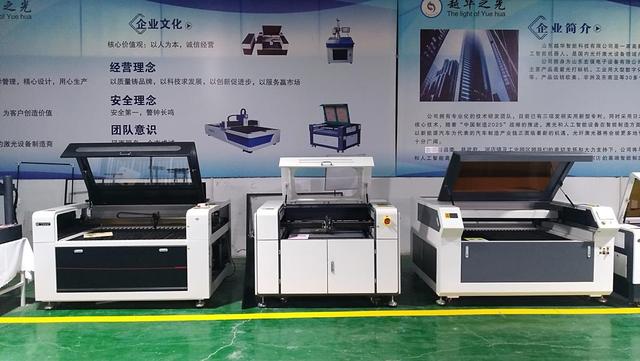
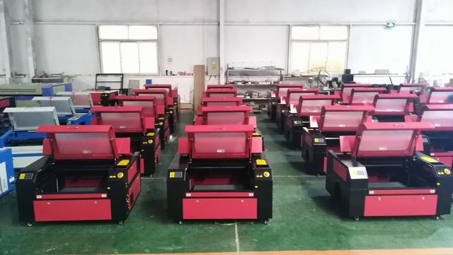
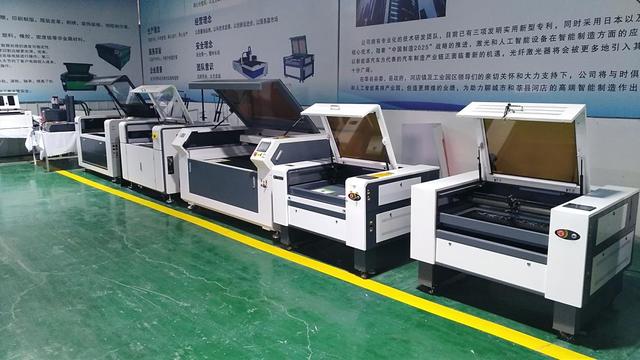
Take a look inside our specialized testing laboratories and high-capacity assembly floor in Hangzhou, China.
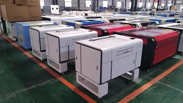
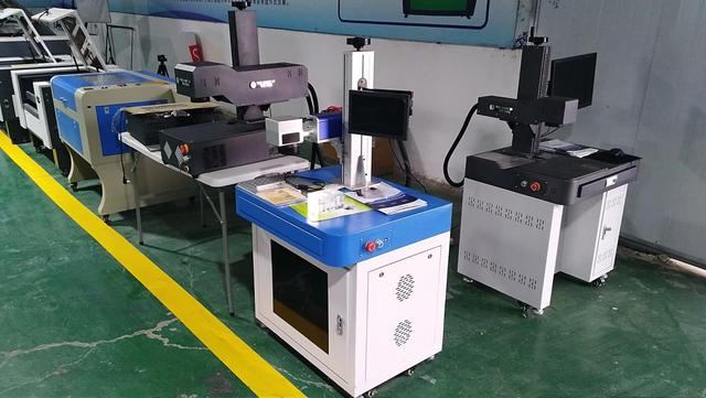
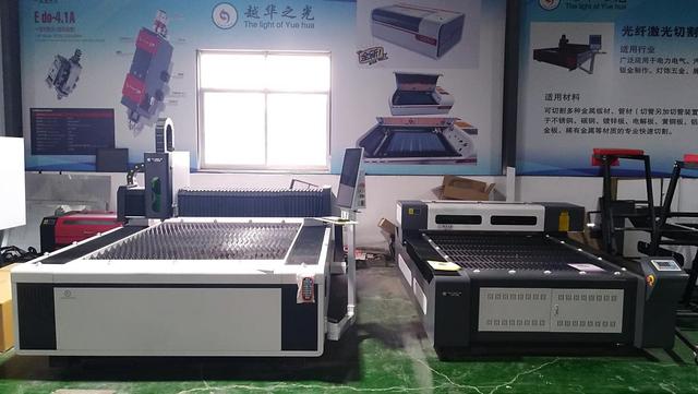
Answers to critical technical queries for manufacturing engineers and procurement heads in Kuala Lumpur.
UV laser marking systems operate at 355nm wavelength, utilizing "cold photo-ablation" techniques. Unlike CO2 (10600nm) and Fiber (1064nm) lasers, which rely on localized thermal energy to melt or burn materials, UV lasers break chemical bonds directly at the molecular level. This results in minimal Heat-Affected Zone (HAZ), preventing copper layer warping, board charring, and micro-delamination on ultra-thin or flexible multi-layer PCB boards.
We provide comprehensive remote configuration support, online diagnostic interfaces, and detailed documentation/video training modules for engineers in Kuala Lumpur. In addition, we coordinate with localized partner technicians in West Malaysia to handle onsite alignment, major maintenance intervals, and emergency replacement component deliveries.
All Kinray machines run on software platforms fully compatible with common design files, including DXF, AI, DWG, PLT, and BMP formats. It communicates easily with manufacturing networks using standard TCP/IP TCP commands, RS232 interfaces, and customized SQL connections, making integration with factory MES/SCADA systems quick and seamless.
Yes. By using our advanced 3W or 5W UV laser systems configured with optimized pulse rates and cooling architectures, the laser vaporizes top film layers safely. It generates high-contrast marks on FPC substrates (like polyimide) without punching through, warping, or damaging the electrical paths underneath.
 Kinray Laser