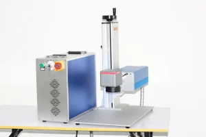
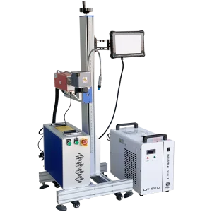
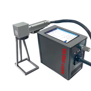
High-end setups designed for strict traceability and micro-marking across Malaysia's leading production floors.
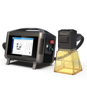
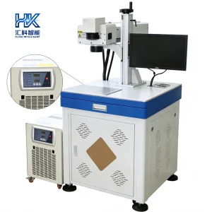
An In-Depth Whitepaper on Micro-processing Dynamics in Penang, Selangor, and Johor Industrial Corridors.
As Malaysia solidifies its position within the global electrical and electronics (E&E) supply chain—handling over 13% of the world's semiconductor back-end assembly, testing, and packaging—the need for extreme traceability tools has intensified. In regions like Penang (Bayan Lepas, Batu Kawan), Kedah (Kulim Hi-Tech Park), and Johor, tier-1 manufacturers and semiconductor packaging houses are transitioning away from thermal-based fiber lasers and mechanical engraving. Instead, the industry is widely adopting 355nm UV (Ultraviolet) Solid-State Laser Marking Systems.
Unlike infrared wavelengths (1064nm) produced by standard fiber lasers, which process materials by heat-induced melting (thermal ablation), UV lasers utilize a "cold marking" photochemical mechanism. The 355nm wavelength has high photon energy capable of breaking chemical bonds directly inside the material's molecular structure. This process produces minimal heat-affected zones (HAZ), eliminating structural warping, micro-cracking, and electrical degradation of adjacent silicon layers or dielectric membranes.
| Parameter | UV Laser (355 nm) | Fiber Laser (1064 nm) | CO2 Laser (10600 nm) |
|---|---|---|---|
| Primary Application | Silicon, Ceramics, Plastics, Glass, FPC | Metals, High-density Plastics | Wood, Acrylic, Paper, Leather |
| Thermal Influence | Negligible (Cold Processing) | High (Thermal Melt) | Extremely High (Carbonization/Burning) |
| Beam Spot Size | <15 μm (Highly Focused) | >50 μm | >100 μm |
| Contrast Ratio on Plastic | High / Structural Contrast | Low / Foaming and Melting | Poor (Typically Engraves Only) |
Modern silicon wafers, integrated circuits (ICs), and thin leadframes require micro-sized, high-density 2D DataMatrix codes. UV lasers generate crisp, ultra-high-resolution marking down to 0.5mm x 0.5mm dimension limits without penetrating deep wafer structures, ensuring zero ESD (Electrostatic Discharge) issues and preserving chip electrical integrity.
Medical manufacturers in Selangor and Johor produce complex catheters, surgical implants, and cleanroom packaging. In compliance with FDA and regional regulatory bodies, these components require permanent Unique Device Identification (UDI) marks. UV lasers achieve high-contrast, permanent marks directly on medical-grade plastics (e.g., PEEK, PTFE) and medical glass without creating surface roughness that could host bacteria.
With the rapid development of Electric Vehicles (EVs) and smart sensing units, Malaysian automotive component assembly plants demand reliable marking on Flame Retardant 4 (FR-4) substrates and flexible printed circuit boards (FPCs). A 355nm UV laser cuts through or marks copper traces and substrates without inducing thermal carbonization, guaranteeing stable insulating values across circuits.
Your Trusted Partner in Advanced Industrial Laser Technologies and Automated Solutions.
Hangzhou Kinray Laser Co., Ltd. is a leading China industrial laser marking machine manufacturer specializing in advanced fiber and UV laser solutions for global manufacturing industries. With a strong focus on innovation, precision, and intelligent manufacturing, Kinray Laser is committed to delivering high-performance laser equipment that improves production efficiency, product traceability, and marking quality.
Located in Hangzhou, China, the company integrates research and development, manufacturing, sales, and technical support to provide comprehensive laser processing solutions for customers worldwide. Our extensive product portfolio includes fiber laser marking machines, UV laser marking machines, CO2 laser marking systems, MOPA laser markers, flying laser marking machines, 3D laser marking equipment, and customized automated laser solutions.
Kinray Laser products are widely used in electronics, automotive, medical devices, precision hardware, jewelry, packaging, aerospace, consumer goods, and industrial manufacturing industries. Designed for high-speed, high-precision, and permanent marking applications, our systems are capable of processing a wide range of materials, including metals, plastics, ceramics, glass, and composite materials.
Equipped with advanced production facilities and rigorous quality management systems, Kinray Laser maintains strict quality control throughout every stage of manufacturing. Each machine undergoes comprehensive testing to ensure stable performance, reliability, and compliance with international standards.
To support global customers, we offer flexible OEM and ODM services for distributors, system integrators, equipment brands, and industrial manufacturers. Our experienced engineering team works closely with customers to develop customized laser solutions tailored to specific production requirements, automation needs, and industry applications.
Driven by technological innovation and customer satisfaction, Hangzhou Kinray Laser Co., Ltd. continues to expand its global presence and strives to become a trusted partner for intelligent laser processing solutions, helping manufacturers achieve smarter, more efficient, and sustainable production.
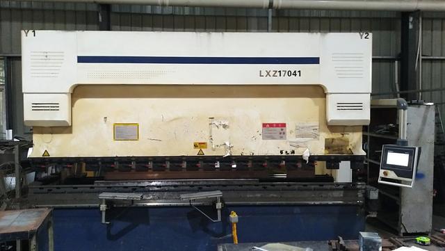
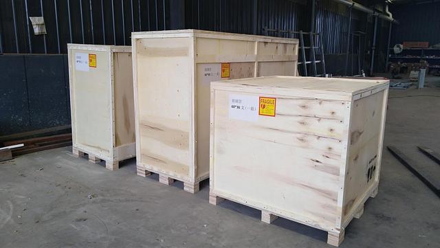
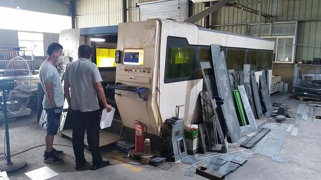
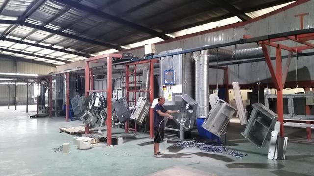
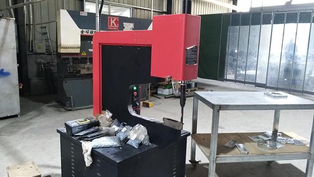
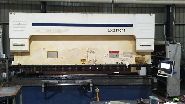
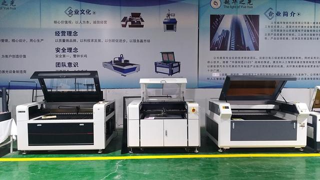
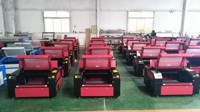
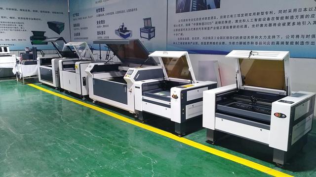
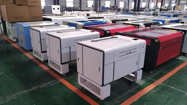
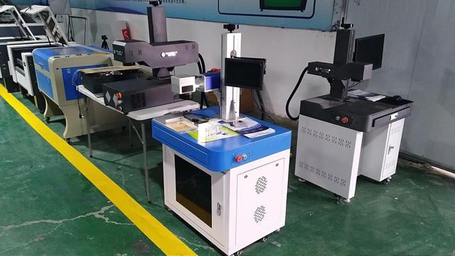
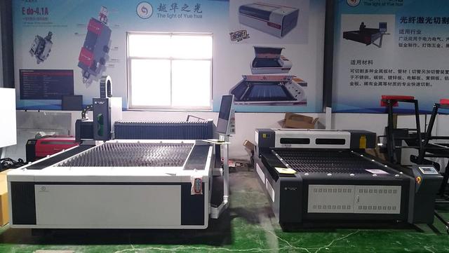
A complete selection of advanced UV and fiber systems configured for heavy industrial applications, including high-speed dynamic tracking and cabinet protection setups.
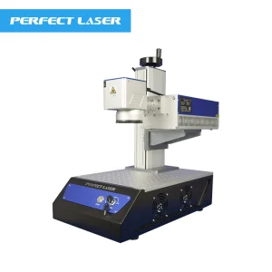
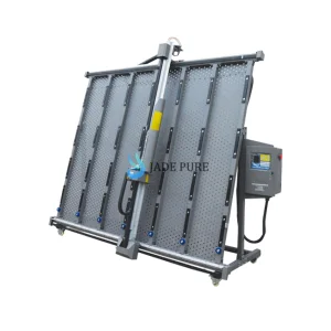
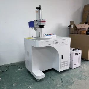
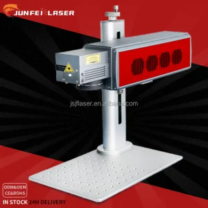
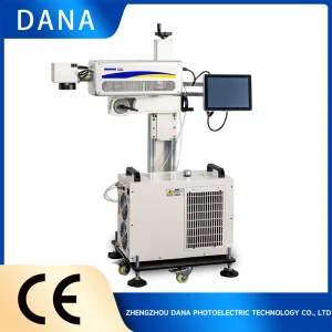
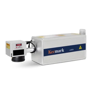
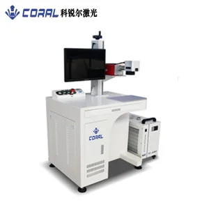
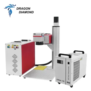
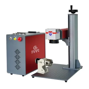
As micro-electronics move toward narrower line widths and 3D stacked chips (such as High Bandwidth Memory, HBM, which is actively packaged in modern Southeast Asian semiconductor centers), UV laser architectures are expanding across three core technology pillars:
Kinray UV Lasers implement high-end JPT and custom-engineered 355nm cavity configurations, combined with f-theta scanning lenses from industry leaders. This ensures stable power density across the entire marking field, preventing peripheral beam distortion.
Technical answers to key inquiries from industrial procurement and manufacturing engineers.
Contact Kinray Laser's optical engineers for parameter consultations, custom configurations, and factory-direct pricing for your facilities in Malaysia.
Send Inquiry Now Kinray Laser